 Coupling & Crosstalk is my column in the MEPTEC Report. This column appears in the Fall 2020 edition on pages 9-10.
Electronic coupling is the transfer of energy from one circuit or medium to another. Sometimes it is intentional and sometimes not (crosstalk). I hope that this column, by mixing technology and general observations, is thought provoking and “couples” with your thinking. Most of the time I will stick to technology but occasional crosstalk diversions may deliver a message closer to home.
Replacing the Road
Hello, fellow road warriors! Do you feel lost? Unappreciated? Unable to deliver your message or solve customer problems? I too am struggling with the current pandemic situation. And I suspect many of you are too – especially the dyed in the wool corporate marketing, sales, and business development road warriors. Truth be told, I Continue reading “Coupling & Crosstalk: Replacing the Road”


 Coupling & Crosstalk is my column in the
 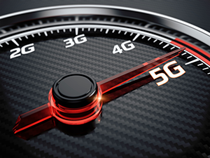 Coupling & Crosstalk is my column in the
  Coupling & Crosstalk is my column in the
  Coupling & Crosstalk is my column in the
  Coupling & Crosstalk is my column in the
 Coupling & Crosstalk is my column in the
  Coupling & Crosstalk is my column in the
  Coupling & Crosstalk is my column in the
  Coupling & Crosstalk is my column in the
  Coupling & Crosstalk is my column in the
  Coupling & Crosstalk is my column in the
  Coupling & Crosstalk is my column in the
  Coupling & Crosstalk is my column in the


 Coupling & Crosstalk is my column in the
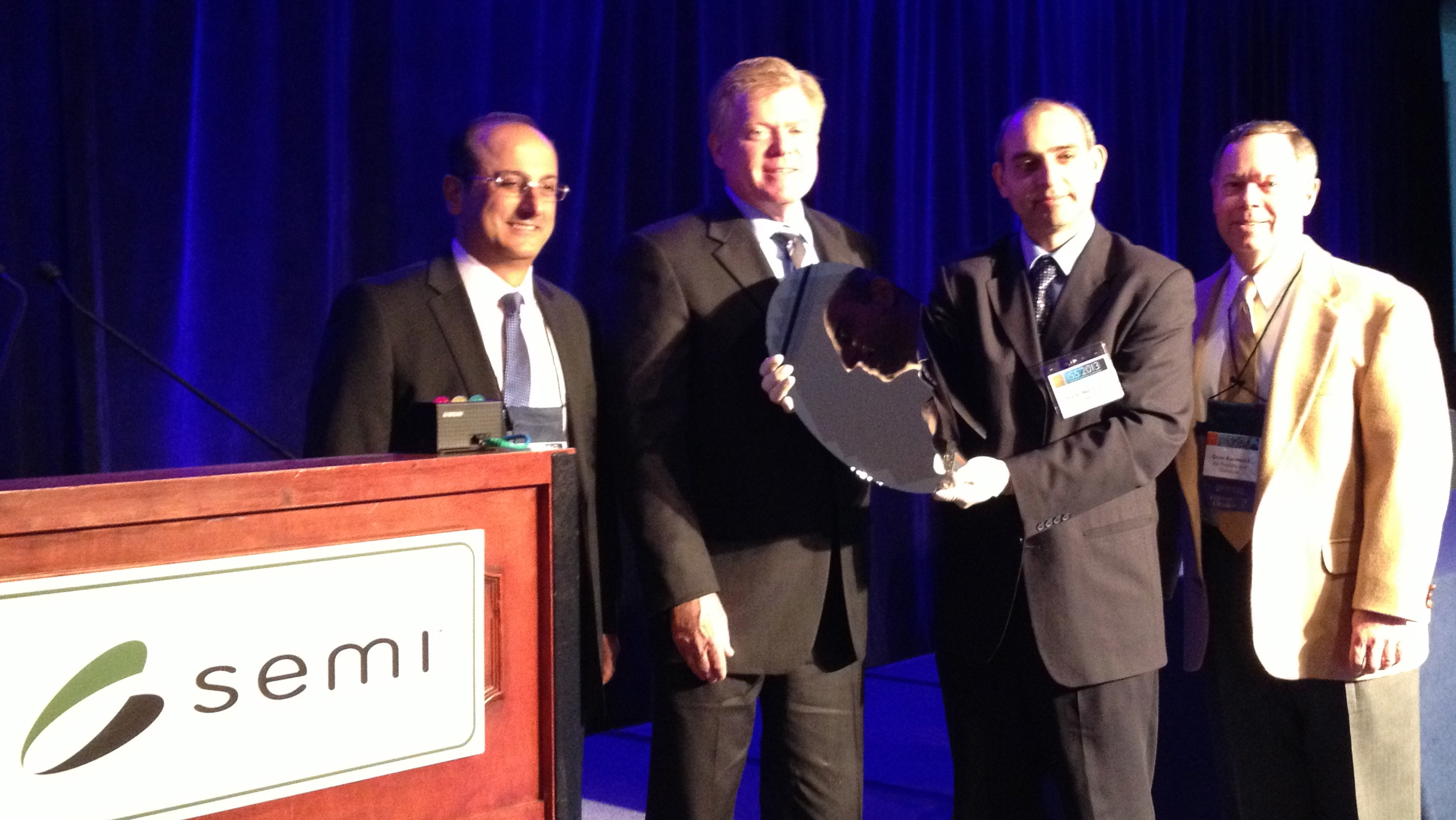


 and Ira Feldman (r) combo headshot 400x200")


 Here are the highlights from Session Nine – “Productivity / COO” of the 21st annual


")


