Coupling & Crosstalk: Headlines, trend lines, or expertise?

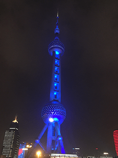
Shanghai Oriental Pearl Radio & TV Tower
 
Coupling & Crosstalk is my column in the MEPTEC Report. This column appears in the Fall 2015 edition on pages 10-11.

 
Electronic coupling is the transfer of energy from one circuit or medium to another. Sometimes it is intentional and sometimes not (crosstalk). I hope that this column, by mixing technology and general observations, is thought provoking and “couples” with your thinking. Most of the time I will stick to technology but occasional crosstalk diversions may deliver a message closer to home.

Headlines, trend lines, or expertise?

The recent stock market sell-off caused significant emotional distress to many investors who were caught off-guard. Looking past “the sky is falling” headlines, what business lessons Continue reading “Coupling & Crosstalk: Headlines, trend lines, or expertise?”

SEMI ISS: Sense of Scale

Intel shows first fully patterned 450 mm semiconductor wafer at SEMI ISS 2013

Attending the SEMI Industry Strategy Symposium (ISS) is like drinking from a fire hose with the additional risk of whiplash. Don’t get me wrong, it is an exquisite fire hose but sometimes the data presented can be overwhelming at this conference of semiconductor supply chain executives. The majority of the attendees and presenters are executives from the SEMI member companies that develop the equipment, materials, processes, and technology used to build, test, and package semiconductors. And the executives present from the semiconductor manufacturers are typically the “end customers”.

The greatest value of SEMI ISS, beyond the networking, is the strategic overview of the entire semiconductor ecosystem. What are the market drivers, the technology needed, and the roadmap status of this industry? It is true that we all know where we need to head courtesy of Moore’s Law and the International Technology Roadmap for Semiconductors which attempts to keep us on that trajectory. The pressure of consumers needing wanting greater functionality at lower costs is relentless. Much of the technological detail of this ecosystem is addressed in a myriad of other forums throughout the year. ISS ties these technical requirements, development needs, and business needs back to the strategic direction and desires of the global marketplace.

The whiplash comes from  Continue reading “SEMI ISS: Sense of Scale”

IEEE Semiconductor Wafer Test Workshop 2012 – Welcome & Session 1 (Monday)

Semiconductor wafer test workshop swtw sign 500x352

Here are the highlights from the Welcome and Session One “Process Improvements for HVM” of the 22nd annual IEEE Semiconductor Wafer Test Workshop (SWTW) from Monday June 11, 2012.

Jerry Broz (SWTW general conference chair) started with several sets of numbers: SWTW attendance (up), semiconductor revenue and wafer statistics (problems). and probe card market (up). The problem with semiconductor statistics are  Continue reading “IEEE Semiconductor Wafer Test Workshop 2012 – Welcome & Session 1 (Monday)”

Two Conferences – Two Industries Challenged By Post PC Era

Tim Cook introducing Apple's latest iPad

The “Post Personal Computer” (Post PC) era became the hot topic when Tim Cook introduced the latest iPad last week. Yes, calling it a “revolution” is definitely hype that is part of Apple‘s Post PC marketing campaign. Hype aside, it is clear that there has been a marked shift in digital hardware for the consumption of content and communication. The PC – be it a Windows, Mac, or Linux based system – is no longer “the device”. It is now one of many devices including portable music players (dominated by iPods), smart phones (lead by iPhones and Android based systems), and tablets (dominated by iPads). The shift is large and the impact is huge. To understand how big, watch the first three minutes of Mr. Cook’s presentation. Then you will understand why Apple had the largest market capitalization of any US company in February – the numbers are staggering.

Even though many were surprised to learn that we are now “Post PC”, some of us who have been developing strategies for the electronic supply chain have Continue reading “Two Conferences – Two Industries Challenged By Post PC Era”

Probe Card Cost Drivers from Architecture to Zero Defects

Click image to download presentation

As the final presenter at this week’s IEEE Semiconductor Wafer Test Workshop (SWTW), I outlined how critical it is to understand the true cost of a product’s architecture in “Probe Card Cost Drivers from Architecture to Zero Defects“. Without a proper understanding of these costs – especially for fully custom high technology products such as wafer test probe cards – it is impossible to maintain a sufficient gross margin. Gross margin is essential to maintain the health of a company and to fund the research & development required for innovation.

Many companies in the semiconductor test market have entered a period that Steve Newberry identified in his 2008 speech “Semiconductor Industry Trends: The Era of Profitless Prosperity?” that parallels the aluminum industry in the 1970’s. And without the means to fund innovation, companies have no future especially when faced with the double threat of Moore’s Law – increasingly harder technical requirements delivered at lower cost.

Yes, there were a few in the audience who appeared pleased since they are confident that their products are on the right path. There were others who may have been upset based upon their company’s direction. I would argue that a proper diagnosis – regardless of how disturbing – is essential to drive the proper cure.

There is plenty of opportunity in the test market and reasons for optimism. The key to long term prosperity is to really understand the fundamentals of the business and not be blinded by the technology.

I thank those who stayed for the entire conference and welcome your thoughts below. And I will be posting more about the conference (including my summaries) in the next few weeks.


Yes, 40%, Most Likely

What does your model say?

What does your model predict?

Even though this sounds like the start of a Carnac the Magnificent comedy act, these are some of the answers from my Probe Card Market model. I keep my model current so I know both industry and company specific performance as well as to make predictions. You don’t have a model? Are you reacting instead of predicting?

So here are the “questions” being answered:

Continue reading “Yes, 40%, Most Likely”

MEMS Technology Summit – Day One – AM (1) – Special Presentations

MEMS Products Phases of Development - Yole Research
Last Tuesday,the MEMS Technology Summit at Stanford University, opened with a welcome by Professor Roger Howe. Roger not only provided a brief history of MEMS at Stanford, he was his characteristic gracious self and welcomed even those with close ties to Berkeley especially the Berkeley Sensor and Actuator Center (BSAC). Truth-be-told even though Roger is a Mudder first, Continue reading “MEMS Technology Summit – Day One – AM (1) – Special Presentations”

Probe Cards & Dart Boards

The wildly varying projections for the semiconductor market in general and the wafer probe market in specific makes me believe that many analysts are simply torn between reporting their tea leaf readings and the scores on their dartboard. A hopefully more reliable source is VLSI Research and their annual probe market survey is eagerly anticipated every spring. One may argue about methodology but on the whole they do an excellent job of painting a comprehensive picture.

Their optimistic forecast is heartening but increased sales volume doesn’t always translate into profits and downturns when they occur can be fatal. Do you prepare for growth like a hare or a tortoise? Do you build excess capacity (“Field of Dreams“), take and fulfill new orders with lots of overtime and temporary workers, or do you forgo new business that bears high incremental start-up costs?

Continue reading “Probe Cards & Dart Boards”