 Coupling & Crosstalk is my column in the MEPTEC Report. This column appears in the Summer 2013 edition on pages 13-14.
Electronic coupling is the transfer of energy from one circuit or medium to another. Sometimes it is intentional and sometimes not (crosstalk). I hope that this column by mixing technology and general observations is thought provoking and “couples” with your thinking. Most of the time I will stick to technology but occasional crosstalk diversions may deliver a message closer to home.
Name Calling
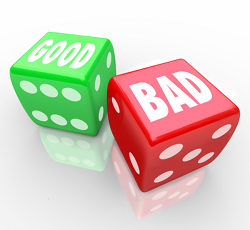
What’s in a name? A lot! A name itself might not mean much but it can trigger expectations and stereotypes. In the United States we have red states and blue states depending on which political party has the majority vote. Similarly, when someone labels themselves on the basis of their political party affiliation (Republican, Democrat, Libertarian, Independent, etc.) others make assumptions how they think about the topical issues of the day.
Names are constructs that enable humans to characterize and build mental constructs and models about our world. Yes, they often lead to (over) simplification however without them the world might be too complex for one to comprehend.
If you have been in the electronic industry long enough, you probably have an opinion on “KGD”. It is not a term widely known outside the world of semiconductors. I’ve heard others think it is a sister organization to the feared Komitet gosudarstvennoy bezopasnosti (KGB). The concept of obtaining known good die (KGD) probably strikes as much fear and loathing in a test engineer or product manager as the KGB did for Soviet dissidents.
There has been plenty of discussion on how to best obtain KGD over the years at test and integrated circuit related conferences. The annual Known Good Die Workshop started in 1994 to focus on the need for KGD driven mainly by the needs of multi chip modules (MCM) at that time. The KGD event is now managed by MEPTEC and was last produced in 2012 where the greater focus was on KGD for 2.5 and 3D integrated circuit (IC) packaging. Hopefully after a hiatus this year, it will be back next year for the 20th anniversary.
Some may argue that true KGD are as mythical as unicorns. They are so elusive that finding a good definition is difficult. (What? There is no Wikipedia entry for KGD? Correct, only a passing mention in the Wafer Testing entry. Please feel free to create an entry.) For argument’s sake, I will offer up my own definition:
A known good die (KGD) is a singulated (diced) integrated circuit that:
- Has been tested and burned-in to a quality level that is sufficient to “know” the die meets all product specifications.
AND
- There is a sufficient confidence will operate correctly and not cause failures when assembled, often irreversibly or without rework/repair possibilities, in a subassembly (MCM, 2.5/3D package, etc.).
Needless to say there are several elements of this definition that are subjective. And an experienced engineer should immediately understand why the quest for KGD is extremely challenging if not downright frustrating.
In the late 1980’s and early 1990’s the KGD user community was a small group typically focused on high performance or high reliability applications such as supercomputing, military or space, implantable medical devices, and automobile safety systems. In our current era of More than Moore applications enabled by advanced 2.5D and 3D packaging, KGD is again a hot topic since the challenge is to integrate bare die and die stacks from multiple suppliers. Neither the integrator (packaging entity) nor the die suppliers want to cause the failure of the entire 2.5D/3D package therefore everyone will claim to ship KGD or known good (sub-)stacks (KGS).
The biggest change since the 1980’s is the demise of vertically integrated electronic supply chains and most suppliers are focused on one part of the supply chain which requires them to obtain material from others. Business models for 2.5D/3D packaging may contain some version of the “blame game”: if your part caused the entire subsystem to fail you need to pay for the cost of all the materials, assembly, and test. With constantly shrinking gross margins, a supplier certainly doesn’t want to absorb the cost of their “failing” part let alone reimburse others therefore the emphasis on claiming KGD/KGS status. And the cost of the integrator or end product company to perform the root cause analysis (RCA) to determine fault is neither trivial nor inexpensive. In some cases, the RCA may be inconclusive or the cost exceed the value of the failing material.
Since KGD are not only elusive but problematic, what can be done to enable electronics to advance? This is a topic that I have discussed often with my colleagues in the Test & Test Equipment Technology Working Group (TWG) of the International Technology Roadmap for Semiconductors (ITRS). We are considering a change in the upcoming roadmap to be published at the end of this year. Though only the roadmap as published by the ITRS is the official opinion of the ITRS team, I feel it is worthwhile to share this thinking.
The change under considered is to replace the term “Known Good Die” with “Not Known Bad Die” (NKBD) or perhaps “Probably Good Die” (PGD). This is intended to be more than a sematic change and to force a change in thinking. Today the downstream user of a die believes it is good, based upon the previous testing. In reality it is very difficult to exhaustively and economically test the die to the full range of specifications. Sometimes the only way to completely test a die is through destructive testing. What typically happens is that a given device passes all the reasonable (and often economical) tests and is shipped having not been found to be bad.
With this shift in terms, the downstream user – die stack integrator, assembler of multichip modules, system designer, etc. – needs to consider how to build subsystems and systems that can be diagnosed for both materials (bad die) and assembly issues. These (sub)systems need to be re-workable, repairable, or disposable (assuming the costs are low enough) in the factory and/or in the field since it cannot be guaranteed that all die are good or will remain so over their life. At the same time it would be well advised to consider how to build systems with greater fault tolerance and self-repair as system complexity continues to increase.
This may sound like a new paradigm for integrated circuits, however dynamic random access memory (DRAM) suppliers have been operating with internal repair for many years. Modern DRAM would have a very low yield (some designs will intrinsically yield no parts) due to defect density versus the size of the die area and the very small feature size of the memory cell. Therefore, DRAMs are tested in the factory and defective bits are switched with spare memory cells using laser or electrical repair. This allows almost all of the DRAM die on a wafer to be used unless there are significant defects.
Even though Not Known Bad Die (NKBD) is a mouthful, it really is more descriptive and should prompt improved system thinking that considers the challenges of developing advanced semiconductors and systems. Let’s clean up our language to communicate today’s reality! Our job as designers, test engineers, product managers, and managers is to work with what we have – even if imperfect – not what we wished we had.
Want to throw out some names or add to this discussion? I welcome your comments below!
